车规级稳压管
产品型号:TPS7B6950DBVR
产品展商:
简单介绍
The TPS7B69xx-Q1 device is a low-dropout linear regulator designed for up to 40-V VI operations. With only 15-µA (typical) quiescent current at light load, the device is suitable for standby microcont
详情介绍
1 Features
-
Qualified for Automotive Applications
-
AEC-Q100 Qualified With the Following Results:
-
Device Temperature Grade 1: –40°C to 125°C Ambient Operating Temperature Range
-
Device HBM ESD Classification Level 2
-
Device CDM ESD Classification Level C4B
-
4 to 40-V Wide VI Input Voltage Range With up to 45-V Transient
-
Maximum Output Current: 150 mA
-
Low Quiescent Current (IQ):
-
15 µA Typical at Light Loads
-
25 µA Maximum Under Full Temperature
-
450-mV Typical Low Dropout Voltage at 100 mA Load Current
-
Stable With Low ESR Ceramic Output Capacitor (2.2 to 100 µF)
-
Fixed 2.5-V, 3.3-V, and 5-V Output Voltage Options
-
Integrated Fault Protection:
-
Thermal Shutdown
-
Short-Circuit Protection
-
Packages:
-
4-Pin SOT-223 Package
-
5-Pin SOT-23 Package
2 Applications
-
Automotive
-
Infotainment Systems With Sleep Mode
-
Always-On Battery Applications
-
Door Modules
-
Remote Keyless-Entry Systems
-
Immobilizers
3 Description
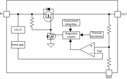
The TPS7B69xx-Q1 device is a low-dropout linear regulator designed for up to 40-V VI operations. With only 15-µA (typical) quiescent current at light load, the device is suitable for standby microcontrol-unit systems especially in automotive applications.
The devices feature an integrated short-circuit and overcurrent protection. The TPS7B69xx-Q1 device operates over a –40°C to 125°C temperature range. Because of these features, the TPS7B6925-Q1, TPS7B6933-Q1, and TPS7B6950-Q1 devices are well suited in power supplies for various automotive applications.
Device Information(1)
|
PART NUMBER
|
PACKAGE
|
BODY SIZE (NOM)
|
TPS7B6925-Q1
TPS7B6933-Q1
TPS7B6950-Q1
|
SOT-223 (4)
|
6.50 mm × 3.50 mm
|
|
SOT-23 (5)
|
2.90 mm × 1.60 mm
|
-
For all available packages, see the orderable addendum at the end of the datasheet.
4 Typical Application Schematic
5 Revision History
Changes from A Revision (December 2014) to B Revision
-
Changed the TPS7B6933-Q1 device status from Product Preview to Production DataGo
-
Added the TPS7B6933-Q1 device test results to the Typical Characteristics sectionGo
Changes from * Revision (November 2014) to A Revision
-
Changed the device status from Product Preview to Production DataGo
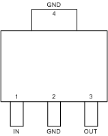
6 Pin Configuration and Functions
DCY Package
4-Pin SOT-223
Top View
DBV Package
5-Pin SOT-23
Top View
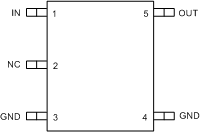
NC - No internal connection
Pin Functions
|
PIN
|
TYPE
|
DESCRIPTION
|
|
NAME
|
NO.
|
|
SOT-223
|
SOT-23
|
|
GND
|
2
|
3
|
G
|
Ground reference
|
|
4
|
4
|
|
IN
|
1
|
1
|
P
|
Input power-supply voltage
|
|
NC
|
—
|
2
|
—
|
Not connected pin
|
|
OUT
|
3
|
5
|
P
|
Output voltage
|